163 lines
4.6 KiB
Markdown
163 lines
4.6 KiB
Markdown
---
|
|
path: /elektro/hr/rts10/
|
|
tags: kladjes, elektro, elektro/hr, elektro/hr/rts10
|
|
auther:
|
|
- Finley van Reenen (0964590@hr.nl)
|
|
auther_short: "E.L.F. van Reenen"
|
|
---
|
|
|
|
# Report Week 1.2
|
|
|
|
## volatile
|
|
|
|
`volatile` is a keyword in c to specify to the comiler it soult not optimize the variable away. This can be usfull for debugging perpeses, if a it is used somewhere the compiler does not reconize or (for example hardwere registers). I learnd this form colleagues on my internship at Erisk.
|
|
|
|
## assignment 2.2
|
|
|
|
> will in line 14 and 21^[line numerbers differ from the assignment, becouse change longer lines te prevent linewrapping] to alternate the green and red with oragne and blue.
|
|
|
|
The pinout is as followed
|
|
|
|
orange: port D bit 13
|
|
green: port D bit 12
|
|
red: port D bit 14
|
|
blue: port D bit 15
|
|
|
|
Bit 12 and 14 sould start different as bit 13 and 15. Then invert all four bits every loop to achees the assignment.
|
|
|
|
I found the defines in the sourcefile where the _modder_ defines are defined.
|
|
|
|
```c-like=
|
|
#include <stdint.h>
|
|
#include <stm32f4xx.h>
|
|
|
|
int main(void)
|
|
{
|
|
// GPIO Port D Clock Enable
|
|
RCC->AHB1ENR = RCC_AHB1ENR_GPIODEN;
|
|
// GPIO Port D Pin 15 down to 12 Push/Pull Output
|
|
GPIOD->MODER = GPIO_MODER_MODER12_0
|
|
| GPIO_MODER_MODER13_0
|
|
| GPIO_MODER_MODER14_0
|
|
| GPIO_MODER_MODER15_0;
|
|
// Set green and red LEDs
|
|
GPIOD->ODR = GPIO_ODR_OD12 | GPIO_ODR_OD14;
|
|
// Do forever:
|
|
while (1)
|
|
{
|
|
// Wait a moment
|
|
for (volatile int32_t i = 0; i < 1000000; i++);
|
|
// Flip all LEDs
|
|
GPIOD->ODR ^= GPIO_ODR_OD12
|
|
| GPIO_ODR_OD13
|
|
| GPIO_ODR_OD14
|
|
| GPIO_ODR_OD15;
|
|
}
|
|
}
|
|
```
|
|
|
|
> How is the assambly generated for line 9 compeard to the magic value `0x55000000`
|
|
|
|
The compiler regonizes that it can calculate the or opperations at compile time becouse it only used compile time defines as inputs. This reults in the foloing line of assambly.
|
|
|
|
```asm
|
|
mov.w r2, #1426063360 @ 0x55000000
|
|
```
|
|
|
|
## assignment 2.3
|
|
|
|
skiped
|
|
|
|
## assignment 2.4
|
|
|
|
skiped
|
|
|
|
## assignment 2.5
|
|
|
|
> Copy the project from assignment 2.2 and update the clock to use the $8 MHz$ external cristal (HSE).
|
|
|
|
I added line 6 throw 15, the rest is uncheached.
|
|
|
|
```c-like=
|
|
#include <stdint.h>
|
|
#include <stm32f4xx.h>
|
|
|
|
int main(void)
|
|
{
|
|
// Enable HSE
|
|
RCC->CR |= RCC_CR_HSEON;
|
|
// Wait until HSE is stable
|
|
while ((RCC->CR & RCC_CR_HSERDY) == 0);
|
|
// Select HSE as the system clock
|
|
RCC->CFGR |= RCC_CFGR_SW_HSE;
|
|
// Wait until HSE used as the system clock
|
|
while ((RCC->CFGR & RCC_CFGR_SWS_HSE ) == 0);
|
|
// Disable HSI
|
|
RCC->CR &= ~RCC_CR_HSION;
|
|
|
|
|
|
// GPIO Port D Clock Enable
|
|
RCC->AHB1ENR = RCC_AHB1ENR_GPIODEN;
|
|
// GPIO Port D Pin 15 down to 12 Push/Pull Output
|
|
GPIOD->MODER = GPIO_MODER_MODER12_0
|
|
| GPIO_MODER_MODER13_0
|
|
| GPIO_MODER_MODER14_0
|
|
| GPIO_MODER_MODER15_0;
|
|
// Set green and red LEDs
|
|
GPIOD->ODR = GPIO_ODR_OD12 | GPIO_ODR_OD14;
|
|
// Do forever:
|
|
while (1)
|
|
{
|
|
// Wait a moment
|
|
for (volatile int32_t i = 0; i < 1000000; i++);
|
|
// Flip all LEDs
|
|
GPIOD->ODR ^= GPIO_ODR_OD12
|
|
| GPIO_ODR_OD13
|
|
| GPIO_ODR_OD14
|
|
| GPIO_ODR_OD15;
|
|
}
|
|
}
|
|
```
|
|
|
|
I mesured the toggle time to be around 1.5 seconsds. This is what is expected.
|
|
|
|
> Make use of the PLL to acheef a CPU clock of $100MHz$.
|
|
|
|
First the power modules needs to be configured to allow for the hige clockspeed.
|
|
|
|
```c-like
|
|
// enable power control
|
|
RCC->APB1ENR |= RCC_APB1ENR_PWREN;
|
|
// set voltage to support 100 MHz
|
|
PWR->CR |= PWR_CR_VOS_0 | PWR_CR_VOS_1;
|
|
```
|
|
|
|
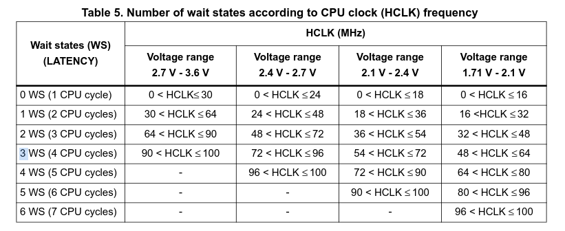
Now the flash latancy is set. The powersupply on the board is $3V$. This means there sould be 3 wait states.
|
|
|
|
|
|
|
|
```c-like
|
|
// set flash latency to support 100 MHz
|
|
FLASH->ACR |= FLASH_ACR_LATENCY_3WS;
|
|
// Wait until the wait states are used
|
|
while ((FLASH->ACR & /* ... */ ) == 0);
|
|
```
|
|
|
|
Finaly we configur the PLL itself.
|
|
|
|
$$
|
|
f_{(VCO\ clock)} = f_{(PLL\ clock\ input)} \cdot (\frac{PLLN}{PLLM}) \\
|
|
f_{(PLL\ general\ clock\ output)} = \frac{f_{(VCO\ clock)}}{PLLP}
|
|
$$
|
|
|
|
$f_{(PLL\ clock\ input)} = 8 MHz$
|
|
$f_{(PLL\ general\ clock\ output)} = 100 MHz$
|
|
$100 MHz \leq f_{(VCO\ clock)} \leq 432 MHz$
|
|
$PLLP \rightarrow \{2, 4, 6, 8\}$
|
|
$50 \leq PLLN \leq 432$
|
|
$2 \leq PLLM \leq 63$
|
|
|
|
Becouse of the liminitan of $PLLP$, $f_{(VCO\ clock)}$ can only be 200 or 400 MHz to acheve the correct $f_{(PLL\ general\ clock\ output)}$.
|
|
|
|
...
|